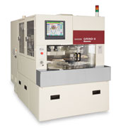
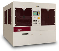
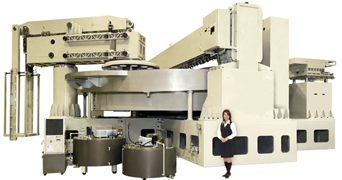
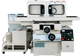
FEATURES Okamoto’s backgrinding, polishing, slicing, and lapping systems are engineered to meet the rigorous demands of advanced material processing and semiconductor manufacturing. Designed for precision and process stability, these platforms deliver tight control over critical parameters such as thickness uniformity, total thickness variation (TTV), surface roughness, and subsurface damage.
With extensive experience across materials including silicon (Si), GaAs, sapphire, quartz, silicon nitride, InP, SiC, and AlTiC, Okamoto systems are optimized to accommodate a wide range of mechanical and thermal properties while maintaining high yield and structural integrity.
Our equipment supports diverse wafer types and device architectures, including SOI, bonded and bumped wafers, as well as advanced processes such as TSV and MEMS. Built for both R&D and high-volume manufacturing, Okamoto platforms emphasize repeatability, automation compatibility, and consistent, high-quality output.
For more information on Okamoto’s full line of Semiconductor Processing Equipment, please contact your local Okamoto Sales Representative.